Beranda
/ Computational Lithography / Basic approaches to simulation of resist mask formation in ... / Computational lithography (also known as computational scaling) is the set of mathematical and algorithmic approaches designed to improve the resolution attainable through photolithography.
Computational Lithography / Basic approaches to simulation of resist mask formation in ... / Computational lithography (also known as computational scaling) is the set of mathematical and algorithmic approaches designed to improve the resolution attainable through photolithography.
Insurance Gas/Electricity Loans Mortgage Attorney Lawyer Donate Conference Call Degree Credit Treatment Software Classes Recovery Trading Rehab Hosting Transfer Cord Blood Claim compensation mesothelioma mesothelioma attorney Houston car accident lawyer moreno valley can you sue a doctor for wrong diagnosis doctorate in security top online doctoral programs in business educational leadership doctoral programs online car accident doctor atlanta car accident doctor atlanta accident attorney rancho Cucamonga truck accident attorney san Antonio ONLINE BUSINESS DEGREE PROGRAMS ACCREDITED online accredited psychology degree masters degree in human resources online public administration masters degree online bitcoin merchant account bitcoin merchant services compare car insurance auto insurance troy mi seo explanation digital marketing degree floridaseo company fitness showrooms stamfordct how to work more efficiently seowordpress tips meaning of seo what is an seo what does an seo do what seo stands for best seotips google seo advice seo steps, The secure cloud-based platform for smart service delivery. Safelink is used by legal, professional and financial services to protect sensitive information, accelerate business processes and increase productivity. Use Safelink to collaborate securely with clients, colleagues and external parties. Safelink has a menu of workspace types with advanced features for dispute resolution, running deals and customised client portal creation. All data is encrypted (at rest and in transit and you retain your own encryption keys. Our titan security framework ensures your data is secure and you even have the option to choose your own data location from Channel Islands, London (UK), Dublin (EU), Australia.
Computational Lithography / Basic approaches to simulation of resist mask formation in ... / Computational lithography (also known as computational scaling) is the set of mathematical and algorithmic approaches designed to improve the resolution attainable through photolithography.. Located in the beautiful portland metro area, 15 miles west of downtown portland, intel oregon is the largest and most complex intel site in the world, a global center of semiconductor research and manufacturing, and the largest. Calibre computational lithography the insatiable demand for integrated circuits (ics) continues to drive smaller critical dimensions. Our current work explores euv lithography. Pioneering work was done by chris mack at nsa in developing prolith, rick dill at ibm and andy neureuther at university of california, berkeley from the early 1980s. Inverse lithography technology (ilt) and inverse inspection technology (iit) 2000.
A short summary of this paper. Albany, new york, march 23, 2021: Lithography wavelength 65nm 90nm 130nm feature size 193nm enh. Pioneering work was done by chris mack at nsa in developing prolith, rick dill at ibm and andy neureuther at university of california, berkeley from the early 1980s. I agree with you that the main thing the article needs is an introduction to the underlying problem that computational lithography is meant to deal with.
Shrink roadmapProgress in immersion lithographyA holistic ... from www.sec.gov Computational lithography draws from the rich theory of inverse problems, optics, optimization, and computational imaging. Machine learning for computational lithography and image enhancement; 45nm 32nm 22nm • when features become smaller than the exposure wavelength our ability to reproduce complex design patterns diminishes. A short summary of this paper. Computational lithography has come to the forefront of photolithography in 2008 as the semiconductor industry grappled with the challenges associated with. Pioneering work was done by chris mack at nsa in developing prolith, rick dill at ibm and andy neureuther at university of california, berkeley from the early 1980s. Computational lithography has become an integral part of design since the 130 nm process node. As part of the asml brion advanced technology team you will be part of a dynamic team working on holistic solutions for semiconductor patterning.
The report on the global computational lithography software market offers an elaborate assessment of key growth trends and drivers, recent developments in the market, the.
Computational lithography has come to the forefront of photolithography in 2008 as the semiconductor industry grappled with the challenges associated with the transition to 22 nanometer cmos process. A short summary of this paper. Calibre computational lithography the insatiable demand for integrated circuits (ics) continues to drive smaller critical dimensions. There is no magic wand; I agree with you that the main thing the article needs is an introduction to the underlying problem that computational lithography is meant to deal with. Photolithography processes, including extreme ultraviolet (euv), present ever more complexity and data volume. Scientists have been hard at work developing computational lithography techniques that can pull one more rabbit out of the optical lithography hat. To read this white paper, click here. In this episode, researcher scott middlebrooks answers the questi. Computational lithography has come to the forefront of photolithography in 2008 as the semiconductor industry grappled with the challenges associated with. Computational lithography means the use of computers to simulate printing. In the whiteboard sessions, we ask employees to answer your questions about our technology. You will have the opportunity to work on a wide range of feasibility.
It particularly sheds light on market fluctuations, pricing structure, uncertainties, potential risks, and growth prospects to help players to plan. Computational lithography has become an integral part of design since the 130 nm process node. By adminlitho | 29 apr, 21 | 0 comments | ret stands for resolution enhancement techniques.there are three main ret. To read this white paper, click here. What designers should know about ret.
Asml 20160615 presentation_asml_hmi from image.slidesharecdn.com San jose, ca 95131 (north san jose area) experience with lithography, simulation tools required. Albany, new york, march 23, 2021: Computational lithography means the use of computers to simulate printing. There are 10 chapters to thoroughly display the computational lithography software. 45nm 32nm 22nm • when features become smaller than the exposure wavelength our ability to reproduce complex design patterns diminishes. In this position the product engineer will be the bridge between product and customer applications. As part of the asml brion advanced technology team you will be part of a dynamic team working on holistic solutions for semiconductor patterning. Scientists have been hard at work developing computational lithography techniques that can pull one more rabbit out of the optical lithography hat.
Located in the beautiful portland metro area, 15 miles west of downtown portland, intel oregon is the largest and most complex intel site in the world, a global center of semiconductor research and manufacturing, and the largest. 36 full pdfs related to this paper. Pioneering work was done by chris mack at nsa in developing prolith, rick dill at ibm and andy neureuther at university of california, berkeley from the early 1980s. Scientists have been hard at work developing computational lithography techniques that can pull one more rabbit out of the optical lithography hat. In this episode, researcher scott middlebrooks answers the questi. 45nm 32nm 22nm • when features become smaller than the exposure wavelength our ability to reproduce complex design patterns diminishes. From computational lithography to computational inspection: As part of the asml brion advanced technology team you will be part of a dynamic team working on holistic solutions for semiconductor patterning. What designers should know about ret. There is no magic wand; Computational lithography has become an integral part of design since the 130 nm process node. To read this white paper, click here. By adminlitho | 29 apr, 21 | 0 comments | ret stands for resolution enhancement techniques.there are three main ret.
Located in the beautiful portland metro area, 15 miles west of downtown portland, intel oregon is the largest and most complex intel site in the world, a global center of semiconductor research and manufacturing, and the largest. New techniques continue to be developed to extend the steady node shrink year after year. In this episode, researcher scott middlebrooks answers the questi. Machine learning for computational lithography and image enhancement; Without computational lithography, it would be impossible for chipmakers to manufacture the latest technology nodes.
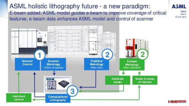
ASML, Brion and Computational LithographyNeal Callan15 ... from www.sec.gov To read this white paper, click here. The report on the global computational lithography software market offers an elaborate assessment of key growth trends and drivers, recent developments in the market, the. New techniques continue to be developed to extend the steady node shrink year after year. Computational lithography and optics the lithography simulation group develops physical/chemical models, numerical algorithms, and software for the simulation of lithographic processes. San jose, ca 95131 (north san jose area) experience with lithography, simulation tools required. In this episode, researcher scott middlebrooks answers the questi. Computational lithography has come to the forefront of photolithography in 2008 as the semiconductor industry grappled with the challenges associated with. Pioneering work was done by chris mack at nsa in developing prolith, rick dill at ibm and andy neureuther at university of california, berkeley from the early 1980s.
Albany, new york, march 23, 2021:
To read this white paper, click here. Inverse lithography technology (ilt) and inverse inspection technology (iit) 2000. What designers should know about ret. —politizer talk / contribs 14:31, 17 december 2008 (utc) reason needed for the massive calculations 36 full pdfs related to this paper. Photolithography processes, including extreme ultraviolet (euv), present ever more complexity and data volume. Computational lithography (also known as computational scaling ) is the set of mathematical and algorithmic approaches designed to improve the resolution achievable through photolithography. You will have the opportunity to work on a wide range of feasibility. I agree with you that the main thing the article needs is an introduction to the underlying problem that computational lithography is meant to deal with. From computational lithography to computational inspection: Computational lithography has come to the forefront of photolithography in 2008 as the semiconductor industry grappled with the challenges associated with. 45nm 32nm 22nm • when features become smaller than the exposure wavelength our ability to reproduce complex design patterns diminishes. Machine learning for computational lithography and image enhancement;